


Choosing a High-Voltage Oscilloscope Probe in Five Minutes
Source: Probemart 2026-04-30 Views: 266
Three basic questions
When visiting the high-voltage probe selection guide, you will be asked three basic questions; these questions determine whether the probe is the correct choice for a specific application.
Q1: What is the DC bus voltage?
The DC bus voltage determines the maximum rated voltage required for the probe used for measurement. For AC line signals, this is the peak-to-peak voltage of the AC line. In switching power devices, the bus voltage is usuallyACthe peak voltage of the full-wave rectified AC line or from the driver's/inverter circuit pulse-width modulation (PWM) signal amplitude.
Q2: What is the semiconductor device material?
Silicon (Si), silicon carbide (SiC) and gallium nitride (GaN) are all common materials used for semiconductor devices, and each material has its own unique requirements for the rise time of switching signals:
1. Si Devices typically cannot handle faster than 10 ns rise times
2. SiC devices have rise times of 3 to 5 ns or slower
3. GaN devices have rise times of about 1 to 3 ns
The larger the voltage swing, the slower the rise time, which helps control EMI。
To measure fast rise times and some harmonics, the probe needs sufficient bandwidth. For example, to measure GaN device gate-drive signal, the required probe bandwidth may approach 1 GHz, while to measure the same GaN the output signal on the device, the required bandwidth may be 700 MHz or even as low as 350 MHz。
Q3: What are the applications?
The high-voltage probe selection guide asks about your measurement application and provides power semiconductor testing, floating sensor, or system input//output measurement options. This high-level classification determines the relative importance of many probe specifications, including voltage range, bandwidth, attenuation, and isolation.
Power semiconductor testing refers to measurements performed on individual power devices. This includes capturing MOSFET/IGBT gate-drive signals and output signals, and then analyzing them. The analysis includes dead-time verification and switching-loss measurement. Depending on the semiconductor device under test, ideal probe characteristics include a wide voltage range, high offset capability, very good CMRR and higher bandwidth.
Floating sensor measurements include probing series or shunt resistors, temperature sensors, or discrete components, etc. This type of application generally requires higher probe isolation because the signals involved are usually small and have large voltage offsets.
System input//output measurement includes line-side AC voltage,DC/DC converter high- and low-voltage input/output, the DC bus, and inverter-driven PWM output; wide voltage range and common-mode range are typical characteristics of probes relevant to this application.
High-Voltage Probe Selection Guide
LeCroy provides this simple method to help you select a high-voltage probe for a specific application. Open the High-Voltage Probe Selection Guide, answer three basic questions, and you will receive a recommendation for a high-voltage probe, along with the rationale behind our selection.
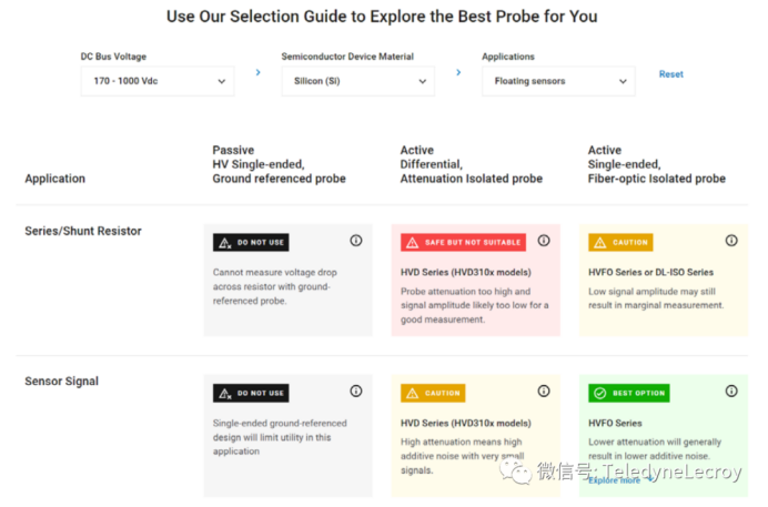
The selection guide uses a simple color-coding scheme to rate the suitability of each probe for the application:
Black:The probe must absolutely not be used for this application, because it may damage the probe, the oscilloscope, or the device under test (DUT), or cause injury to the operator.
Red:Using the probe in this application may be safe, but it may not provide good measurement results.
Yellow:In this application, there are some compromises in probe performance, but some users may find these probes suitable for them.
Green:This is the perfect probe; there are almost no issues with its use, and it is optimized for this application in terms of price and performance. Sometimes, it may be the only safe choice.
Let us look at how to use the High-Voltage Probe Selection Guide to select a suitable probe for testing power semiconductors using a 260 V DC bus.
Example of Selecting the Correct High-Voltage Probe
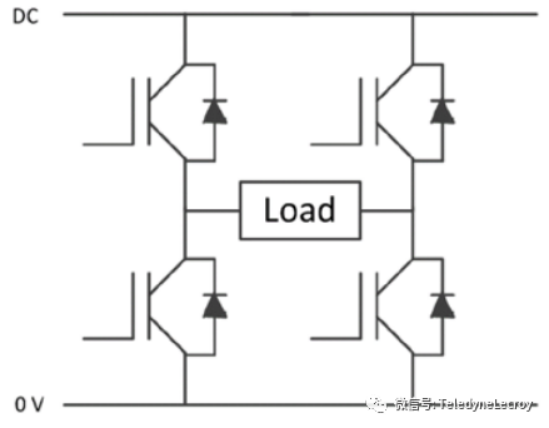
The circuit to be tested is a full-bridge topology using four wide-bandgap (in this case, GaN) metal-oxide-semiconductor field-effect transistors (MOSFETs). What needs to be measured is the switching loss of the MOSFETs. There are two low-side MOSFETs and two high-side MOSFETs, as shown in the figure below.
Based on the above information:
1. The DC bus voltage is selected as 170 – 1000 Vdc
2. The semiconductor device material is selected as wide-bandgap (SiC or GaN)
3. The application is selected as power semiconductor testing.
Then enter this information into the high-voltage probe selection guide, as shown in the figure below.
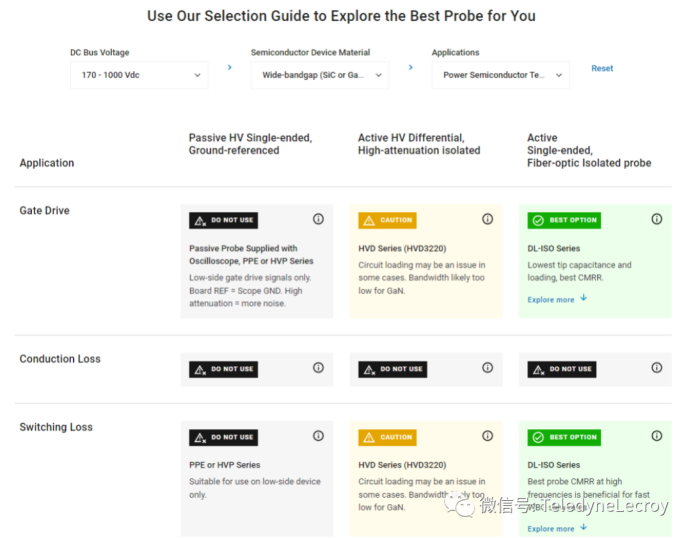
01 Consider the probe requirements of different applications.
The results are displayed in a matrix showing the subcategories of the applications considered and the HV probes considered for each application.
In this example, the high-voltage probe selection guide selects the DL-ISO series high-voltage optically isolated probe as the best probing option for gate-drive and switching-loss measurements (green).
The DL-ISO is a new type of probe designed specifically for measuring small signals floating on a high-voltage DC bus; it has optically isolated characteristics similar to Tektronix IsoVu. The HVD series high-voltage differential probes are high-quality high-voltage differential probes with a conventional design; the selection guide indicates that these probes may be usable (yellow).
The annotations accompanying each option provide a brief rationale for the result, and more information is provided behind the button labeled "i".
Q: Why do power semiconductor device measurements face significant challenges, and why chooseDL-ISOprobe?
1. Measuring low-side MOSFETs is relatively easy because they are ground-referenced. A single-ended passive probe can be used, but it is not recommended because it is easy to accidentally probe the high-voltage (HV) portion of the circuit, thereby damaging the probe, oscilloscope, or device under test (DUT), or injuring the operator.
2. Measuring high-side MOSFETs is more difficult because they are referenced to a nonzero voltage. This is called a floating measurement. This rules out ground-referenced single-ended probes because they would short the DUT. This measurement requires a high-voltage differential or single-ended isolated probe.
3. High-side MOSFET measurements benefit from the high CMRR of optically isolated probes (such as the DL-ISO), which helps eliminate switching interference from the low-side device.
4. When measuring wide-bandgap devices (e.g., GaN and SiC), high bandwidth is also required to accommodate the faster rise times supported by these devices.
Measuring both the high-side and low-side MOSFETs provides a comprehensive understanding of system behavior. In addition to evaluating switching loss, designers will evaluate timing to determine whether the high-side and low-side devices could turn on simultaneously, which would cause a short circuit (shoot-through). Therefore, a probe capable of adequately performing high-side measurements is essential.
For floating measurements on the high-side MOSFET, a single-ended passive probe is a poor choice (black); it poses a safety hazard when used in a floating circuit environment, which is why it is assigned the black classification.
The HVD probe is a better choice than a passive probe, but due to its input capacitance, it may load the circuit more heavily. It may also not have sufficient bandwidth for faster wide-bandgap devices, especially the GaN devices used in the example. Using this type of probe involves some trade-offs, but some users may find that these probes meet their specific measurement needs well.
One reason the DL-ISO is the best choice is the probe's CMRR. The DL-ISO series has a CMRR of 160 dB at DC, and its CMRR at higher frequencies is also significantly higher than that of other probes. The HVD probe has a CMRR of 85 dB at DC and 65 dB at 1 MHz. Although the HVD series probes have excellent CMRR compared with conventional HV differential probes, and their performance can be acceptable depending on the device and circuit, their CMRR is not as good as that of the DL-ISO, and their bandwidth is far below 1 GHz.

Finally, the DL-ISO series probes provide bandwidth up to 1 GHz, which can meet the requirements of GaN devices. The HVD series probes have a maximum bandwidth of 400 MHz, which is closer to the bandwidth requirements of SiC or silicon (Si) power semiconductor devices.
The best choice for this type of power device measurement is a single-ended fiber-optic isolated probe. Its single-ended configuration minimizes loading, thereby providing better signal fidelity. The probe's isolation circuit is less susceptible to transients. It has better CMRR at high frequencies, which is important for circuits using wide-bandgap semiconductors (such as the GaN MOSFET in this example). Combined with the probe's isolation circuit, this enables more accurate high-side measurements.
02 Actual Test Comparison
To demonstrate this, let us compare the Vds (MOSFET drain-source) signals captured with the DL-ISO probe and the HVD probe. The DL-ISO probe (red waveform in the figure below) is connected to the gate of a high-side MOSFET. The HVD probe (blue trace) is connected to the gate of another high-side MOSFET. Simultaneous observation is possible, and the probes do not affect each other by loading the circuit, as would occur if they were connected to the same measurement point.
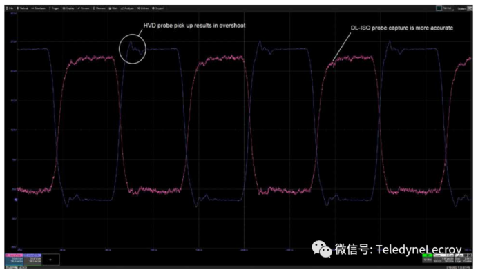
Note that the HVD probe exhibits a small overshoot on edge transitions. This overshoot is likely because the HVD probe has a lower CMRR than the DL-ISO. There is no obvious overshoot in the DL-ISO probe signal; the optical coupling of the DL-ISO probe provides the best CMRR performance, helping to suppress the effects of transients from elsewhere in the circuit.
Reprinted from 力科测试科技

PCIM Europe 2026, Nuremberg: IWATSU and PMK at Booth H7-157
2026-06-15
APEC 2026: 41st IEEE Applied Power Electronics Conference and Exposition
2026-03-15
Semicon China 2026, Shanghai New International Expo Centre (SNIEC)
2026-03-11
WiPDA Asia 2025, Beijing International Convention Center, 15 August
2025-08-06