


Probe Characteristics
Source: Probemart 2024-07-25 Views: 1168
First, it must be recognized that even if the probe is only a simple piece of wire, the probe can still be a very complex circuit. For DC signals (0 Hz frequency), the probe appears as a pair of simple wires with a certain series resistance and termination resistance (Figure 4a). However, for AC signals, as the signal frequency increases, the graph changes markedly (Figure 4b).
With good probe design, the probe's resistance, inductance, and capacitance elements can be controlled to provide the desired signal fidelity, attenuation, and source loading over a specified frequency range. However, even with good design, the probe is still limited by its circuit characteristics. When selecting and using a probe, it is necessary to understand these limitations and their effects.
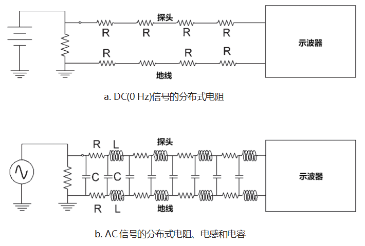
Figure 4 The probe is a circuit composed of distributed resistance, inductance, and capacitance (R, L, and C) elements
Bandwidth and rise time limitations
Bandwidth is the frequency range over which an oscilloscope or probe is designed to operate.
Generally, for accurate amplitude measurements, the oscilloscope bandwidth should be five times higher than the frequency of the waveform under test. This “five-times rule” ensures sufficient bandwidth for the high-frequency components in non-sinusoidal waveforms, such as square waves.

Figure 5 The probe and oscilloscope are designed according to specifications for measurements within the operating bandwidth. At frequencies beyond the 3 dB point, the signal amplitude becomes severely attenuated, and the measurement results may become unpredictable
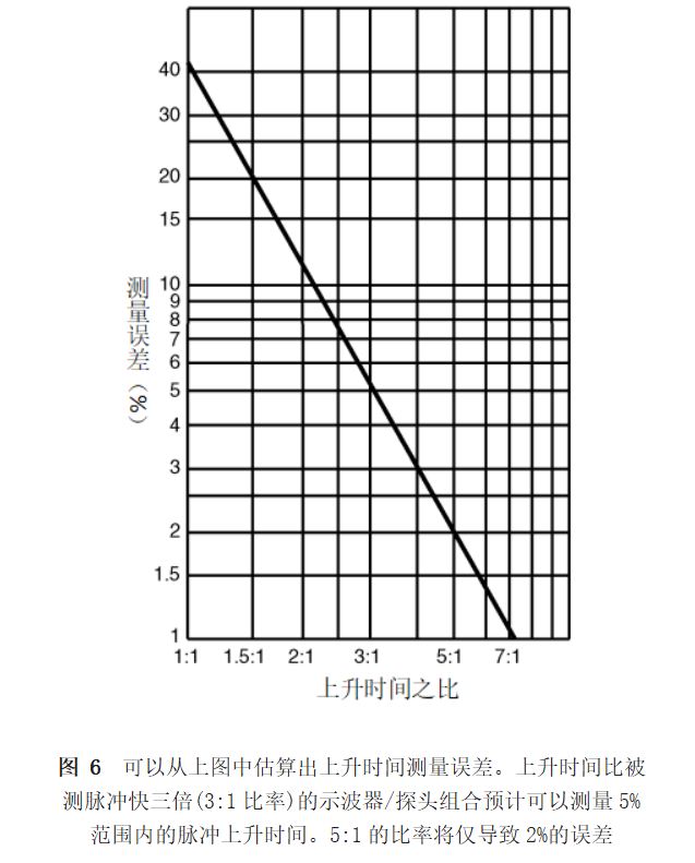
Similarly, the oscilloscope must provide sufficient rise time for the measured waveform. The rise time of an oscilloscope or probe is defined as the rise time measured when using an ideal instantaneous rising pulse. To achieve reasonable accuracy when measuring the rise time or fall time of a pulse, the total rise time of the probe and oscilloscope should be 3–5 times faster than that of the pulse under test (Figure 6).
When rise time is not specified, the following formula can be used, fromBandwidth (BW) Rise time (Tr) derived from the specification:
Tr = 0.35/BW
Each oscilloscope has specified bandwidth and rise-time limits. Similarly, each probe has its own set of bandwidth and rise-time limits. In addition, when a probe is connected to an oscilloscope, a new set of system bandwidth and rise-time limits results.
Unfortunately, the relationship between the system bandwidth and the bandwidths of the individual oscilloscope and probeis not simple, and the same is true for rise time. To address thisproblem, when an oscilloscope is used with a specified probe model, the manufacturer of a high-qualityoscilloscope specifies the bandwidth or rise time at the probe tip. This is very important because, when the oscilloscope and probe are used together, they form a measurement system, and the system bandwidth and rise time determine the measurement capability. If the probe used is not on the oscilloscope manufacturer's list of recommended probes, you may obtain unpredictable measurement results.
Dynamic range limitations
All probes have high-voltage safety limits that should not be exceeded. To avoid personal injury and possible probe damage, it is best to know the voltage under test and the voltage limit of the probe used.
In addition to safety considerations, the dynamic range of the measurement must also be considered in practice. Oscilloscopes have an amplitude sensitivity range. This assumes at least the use of4a signal display in divisions of amplitude to obtain reasonable measurement resolution. In 1X probe (1× probe) in which the dynamic measurement range is the same as that of the oscilloscope. For the above example, the signal measurement range is4 mV - 40 V。
signal-source loading. As previously mentioned, the probe must sink part of the signal current to develop the signal voltage at the oscilloscope input. This presents a load at the test point and may change the circuit or the signal delivered by the signal source to the test point.
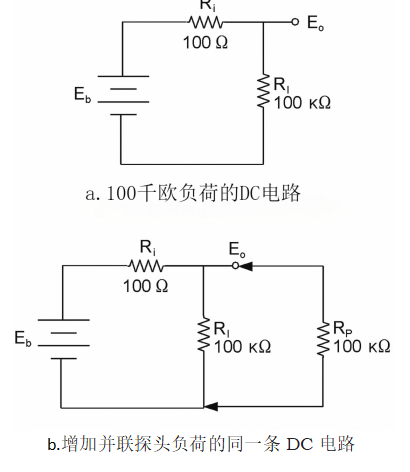
Figure 7 Resistive loading example
The simplest example of source loading effect is a battery-operated resistor network measurement, as shown 7 in Fig. 7a . In Fig. 7a, before the probe is connected, the battery's DCvoltage is divided between the battery's internal resistance (Ri) and the battery-driven load resistance (Ri). For the values given in the figure, the resulting output voltage is:
Eo = Eb * RI/( Ri + RI )
= 100 V * 100,000/(100 + 100,000)
= 10,000,000 V/100,100
= 99.9 V.
In Fig. 7b , the probe has been connected to the circuit, resulting in a probe resistance (Rp) in parallel withRI. If Rp is 100 kW, then in Fig. 7b the effective load resistance is reduced by half, to 50 kW。
ThisEo load effect is:
Eo = 100 V * 50,000/(100 + 50,000)
= 5,000,000 V/50,100
= 99.8 V
The load effect at 99.9 differs from that at 99.8 by only 0.1%, which is negligible for most purposes. However, if Rp is relatively small, such as 10 kΩ, this effect can no longer be neglected.
To minimize this type of resistive loading,1X probes typically have 1 MΩ of resistance,10X probes typically have 10 MΩ of resistance. In most cases, these values cause almost no resistive loading. However, when measuring high-resistance signal sources, some loading should be expected.
Usually, the loading of greatest concern to users is the loading caused by capacitance at the probe tip (see Figure 8).At low frequencies, this capacitance has a very high reactance and has little or no effect. As frequency increases, however, the capacitive reactance decreases. As a result, loading increases at high frequencies.
This capacitive loading affects the bandwidth and rise time characteristics of the measurement system because it reduces bandwidth and increases rise time.
By selecting probes with low tip capacitance, capacitive loading can be minimized. The following table provides some typical capacitance values for various probes:


Figure 8 ForACsignal sources, probe tip capacitance (Cp) is what users are most concerned about
loading. As signal frequency increases, capacitive reactance (Xc) decreases, causing more
signal to flow through the capacitor
To avoid grounding problems, always use the shortest ground lead supplied with the probe. Alternative grounding methods may cause ringing on the pulse under test.
A probe is a sensor
When dealing with the practical characteristics of oscilloscope probes, it is important to remember that a probe is a sensor. Most oscilloscope probes are voltage sensors. That is, they sense or probe voltage signals and transmit the voltage signal to the oscilloscope input. However, other probes allow you to sense phenomena other than voltage signals.
In addition, oscilloscope voltage probes can be used with various other sensors or transducers to measure different phenomena. For example, a vibration transducer allows you to view mechanical vibration signals on the oscilloscope screen. This depends on the types of transducers available on the market.
In any case, however, the combination of transducer, probe, and oscilloscope must be considered a measurement system. In addition, the practical probe characteristics discussed above can also extend to transducers. Transducers also have bandwidth limitations that may cause loading effects.
How can common probing problems be avoided?
It is best to check probe compensation when changing the probe tip adapter.
Use the appropriate probe tip adapter whenever possible.
The ground lead should be asshort and straight as possible
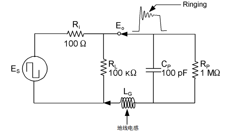
Figure 9 The probe ground lead adds inductance to the circuit. The longer the ground lead, the greater the inductance, and the higher the likelihood of seeing ringing on fast pulses
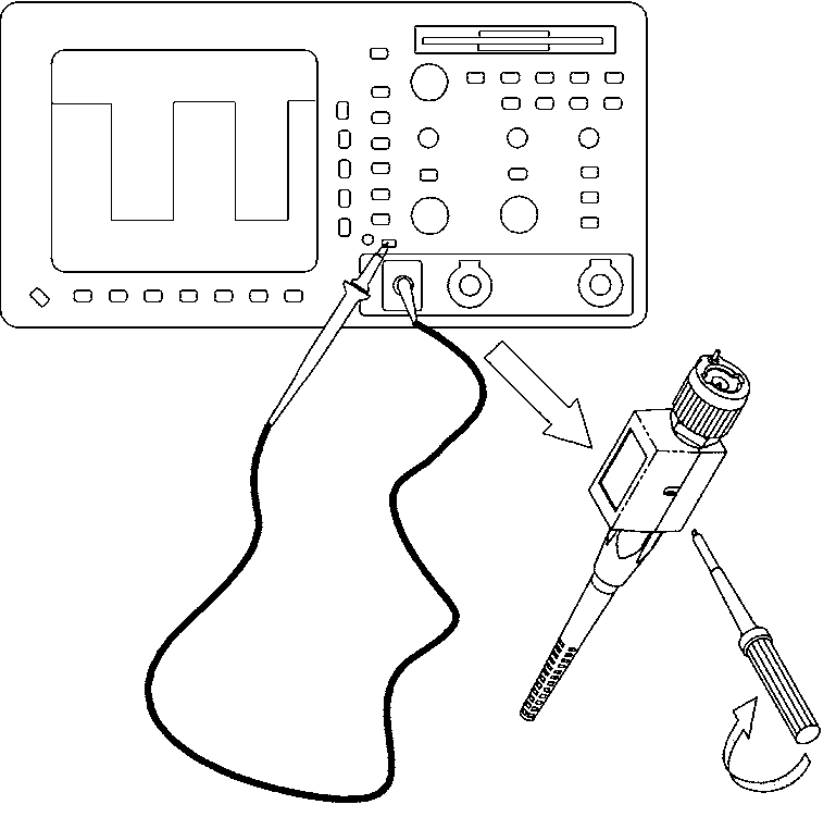
Figure 10 Adjust probe compensation at the probe head or on the compensation fixture connected to the oscilloscope input
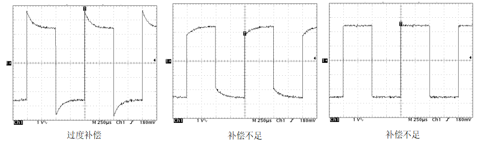
Figure 11 Example of the effect of probe compensation on a square wave

Figure 12 Even a short length of wire soldered to the test point can cause signal fidelity problems. In this case, the rise time from 4.74 ns (a) to 5.67 ns (b)
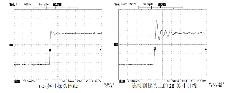
Figure 13 Extending the probe ground lead length can cause ringing on pulses
Reprinted from Tektronix, Those Question Marks About Probes

PCIM Europe 2026, Nuremberg: IWATSU and PMK at Booth H7-157
2026-06-15
APEC 2026: 41st IEEE Applied Power Electronics Conference and Exposition
2026-03-15
Semicon China 2026, Shanghai New International Expo Centre (SNIEC)
2026-03-11
WiPDA Asia 2025, Beijing International Convention Center, 15 August
2025-08-06