


Selecting a Power-Device Dynamic Parameter Test System: Avoiding the Pitfalls
Source: Probemart 2026-05-22 Views: 152
According to the package type of the device under test, power device dynamic parameter test systems fall into two main categories: those for discrete devices and those for power modules. For a long time, test systems for power modules have occupied the vast majority of the market share, while test systems for discrete devices have less demand and limited choices.As the localization of power devices in China accelerates, power device manufacturers and system application companies are paying increasing attention to dynamic parameter testing of power devices, and are placing increasing demands on test systems for discrete devices in particular.
Across the power device dynamic parameter test systems currently available on the market, technology and service levels are uneven. Actual test results very often fail to meet the datasheet, and some test systems do not even have basic test functions, causing users to waste money as well as a great deal of time and effort.
To prevent the above problems from happening again to engineers, this article will walk readers through how to avoid pitfalls when selecting a power device dynamic parameter test system.
01 Test voltage and current ranges to be met
When selecting a test system, the first issue we face is the voltage and current ranges of the device that the test system can test. Test system specifications generally state “maximumxxxV / xxxA”, but such a way of stating specifications is far from sufficient; there are cases where the maximum current cannot be reached at voltages below the maximum voltage.
Assume the load inductance in the test isL, the bus capacitance isC, the test voltage isV, the test current isI, then the double-pulse first1pulse width τ, and the second1pulse width at the end of which the bus voltage drop ratio is less thanKvThe following must be satisfied:

It can be seen that τ is used to make the current reachI, τ increases asIandLincrease, and decreases asVincreases. In actual testing, the τ duration should not be too long; otherwise, device heating will seriously affect the test results. At the same time,Cmust be greater than a certain value to ensure that at the1end of the pulse width, the bus voltage drop ratio is less thanKv, so as to ensure that at the2pulse, the bus voltage drop is within an acceptable range; otherwise, the turn-on and turn-off voltages in double-pulse testing will be inconsistent.Cincreases withIandLincreases with the increase of, and withVandKvdecreases with the increase of. During testing,CandLare determined by hardware conditions,Vis specified by the test conditions; an upper limit is also required for τ, and these parameters together determine the achievable test current.
For high-voltage devices, assumeC=40uF, capacitor voltage rating1100V、L=10uH/50uH/100uH, upper limit of τ, τmax; for low-voltage devices, assumeC=3000uF, capacitor voltage rating200V、L=10uH/50uH/100uH, τ. Based on the formula above, the maximum current that can be achieved at this time is shown in the following figure.

High-voltage devices at400Vtest conditions, with load inductance selected as100uHcan reach36A, selecting50uHcan reach51A, selecting10uHcan reach100Aand above; at800Vtest conditions, load inductance selection of100uHcan reach72A, selecting50uHcan reach101A, selecting10uHcan reach200Aand above.
Low-voltage devices at20Vtest conditions, load inductance selection of100uHonly4A, select50uHonly8A, select10uHcan reach40A; at150Vunder test conditions, with load inductance selected as100uHcan reach30A, select50uHcan reach60ASelect10uHup to300A。
For high-voltage devices, to meet high-voltage test requirements, a bus capacitor with a high voltage rating must be selected, but such capacitors have small capacitance. If this capacitor is used to test low-voltage devices, the maximum current that can be achieved will be greatly reduced. For power devices, voltage rating and on-resistance are in a trade-off relationship; low-voltage devices often require a larger test current, so low-voltage devices should use a bus capacitor with larger capacitance. In addition, as shown in the figure above, at the same test voltage, the smaller the load inductance, the larger the maximum current that can be achieved. To meet the high-current requirements of low-voltage devices, a load inductance with smaller inductance should also be selected.
It can be seen that the maximum test current achievable by the test system is determined byC、L、V, τmaxjointly. When selecting a test system, users can calculate using the above method to check whether it can meet the test requirements.
02 Supported device package types
For a long time, there have been few options for test systems for discrete devices. One reason is that the many package types of discrete devices lead to high development and hardware costs, especially for surface-mount packaged devices. Most test systems on the market only supportTO-247、TO-220such through-hole devices, and cannot test devices in other package forms, which greatly limits the application scenarios of the test system.
To address this issue, the power device dynamic parameter test system introduced by TektronixDPT1000Auses an adapter board to meet the test requirements of discrete devices in most package forms. The adapter board usessocketfor electrical connection to the device; the adapter board is then inserted into thesocketon the test circuit, enabling convenient and rapid replacement of the device under test and different packages.

03 test voltage and current ranges to be met
Suitable measuring instruments are the basis for a test system to obtain accurate test results, mainly including oscilloscopes, voltage probes, and current probes. We can see that some test systems have major problems in the selection of measuring instruments, for example:
Using a basic oscilloscope to measure high-speedMOSFET, high-speedIGBT、SiC MOSFET, because the bandwidth and sampling rate are severely insufficient, the test results deviate greatly from the actual values
Using an oscilloscope with anADCbit depth of8bitto measure high-voltage, high-current devices; due to low resolution, the measured values have poor accuracy
Using a high-voltage differential probe to measure the gate-drive waveform causes high waveform noise and severe ringing. Using a Rogowski coil to measureSiC MOSFETterminal current; because the bandwidth is severely insufficient, the test results deviate greatly from the actual values
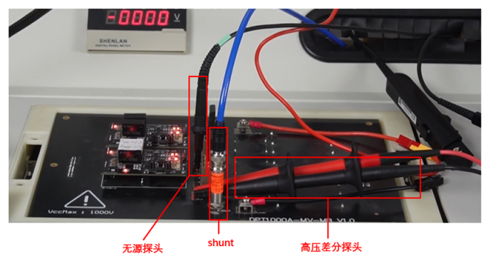
For the characteristics of the measured signals, Tektronix, in the power device dynamic parameter test systemDPT1000Aselected and used appropriate measurement instruments to improve the accuracy of test results.The oscilloscope selected isMSO5Bseries, with a maximum bandwidth up to2GHz, record length up to500Mand features12bitADC, which can meet the bandwidth requirements of high-speed switching and has a higher sampling rate, lower noise, and higher vertical resolution. For gate waveform measurement, a passive probe is used, with bandwidth up to1GHz, low attenuation ratio, and featuresMMCXinterface, enabling accurate measurement of the low-side drive voltage and reducing the influence of the ground lead.
For terminal voltage measurement, a high-voltage differential probe is used; while meeting a wide voltage measurement range, it has higher input impedance, providing safe measurement assurance. For terminal current testing, ashuntresistor is used, with a bandwidth up to1GHzand above, which can meet the bandwidth requirements of high-speed devices.
04 high-side test capability
Double-pulse testing uses a half-bridge inductive-load circuit, and it is sometimes necessary to measure the high-side device. Many test systems use a high-voltage differential probe to measure the high-side device gate-drive signal; the measured waveform often exhibits severe ringing, especially when testing high-speedMOSFET, high-speedIGBT、SiC MOSFETthe situation is even more severe.
This situation is caused by the severe degradation of the common-mode rejection ratio of the high-voltage differential probe at high frequencies; in this case, the test system is in fact not capable of testing the high-side device.
SolvingSiC、GaNthe magic wand for gate dynamic testing challenges
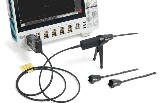
dynamic parameter test systemDPT1000Ain which Tektronix'sIsoVuoptically isolated probe is used to test the high-side device.IsoVuThe optically isolated probe has a common-mode voltage of up to ±60kV, and the differential signal can be as high as ±2000V, and the bandwidth can be as high as1GHz, while also providing an excellent common-mode rejection ratio; at1GHzit can still reach-90dB. Such excellent characteristics ensure the capability to test the high-side device.
05 Loop inductance of the main circuit and gate-driver circuit
In the test circuit, there are two critical loops, namely the main circuit loop and the gate-driver circuit loop. Their impact on the dynamic characteristics of the device is significant, and they are also key indicators for evaluating the performance of the test circuit. Conventional power devices have relatively slow switching speeds, so the requirements on the parasitic inductance of the above two loops are not high. However, with high-speedMOSFET, high-speedIGBT、SiC MOSFETappearing, the problem of large loop inductance in the previous power-device dynamic parameter test system has become apparent.
Specifically, when the main circuit loop inductance is too large, it will cause the turn-off voltage overshoot across the device to be too high. When it exceeds the device voltage rating, it may cause overvoltage damage to the device. When the gate-driver circuit loop inductance is too large, it will cause severe oscillation in the gate-drive waveform, and the gate-driver loop is also susceptible to the highdi/dtinterference, further exacerbating oscillation, possibly causing device gate overvoltage breakdown and device false turn-on that leads to bridge-arm shoot-through.

dynamic parameter testing systemDPT1000ATo address this issue, the test circuit parameters were optimized to enable measurement includingSiC MOSFEThigh-speed devices. The drive circuit is placed close to the device under test and usesPCBrouting connections, minimizing the drive-circuit loop inductance as much as possible. At the same time, in the selection of the DC-link capacitor,PCBrouting and current-sampling method were optimized, further reducing the main-circuit loop inductance.
Reprinted from Tektronix

PCIM Europe 2026, Nuremberg: IWATSU and PMK at Booth H7-157
2026-06-15
APEC 2026: 41st IEEE Applied Power Electronics Conference and Exposition
2026-03-15
Semicon China 2026, Shanghai New International Expo Centre (SNIEC)
2026-03-11
WiPDA Asia 2025, Beijing International Convention Center, 15 August
2025-08-06