


Solving Grounding Problems
Source: Probemart 2025-11-10 Views: 769
Because it is difficult to determine a true ground reference point for a measurement, ground-lead issues still must be considered in oscilloscope measurements. This difficulty stems from the fact that whether the ground lead is on the probe or in the circuit, it has inductance; as signal frequency increases, it becomes its own circuit—that is, a long ground lead causes ringing on pulses. In addition to being a source of ringing and other waveform distortion, the ground lead also acts as a receiving antenna for noise.
To prevent ground-lead problems, first make an assessment. Any noise or distortion observed on the signal display screen should always be suspect. The noise or distortion may be part of the signal or may be a result caused by the measurement process. The following discussion provides relevant information and guidelines to determine whether distortion is part of the measurement process and, if so, how to address this problem.
Ground-lead length
Any probe ground lead has some inductance; the longer the ground lead, the greater the inductance. When combined with the probe-tip capacitance and the signal-source capacitance, the ground-lead inductance forms a resonant circuit that causes ringing at certain frequencies.
To observe ringing or other distortion caused by poor grounding, the following two conditions must be present:
1. The oscilloscope system bandwidth must be high enough to handle the high-frequency components of the signal at the probe tip.
2. The input signal at the probe tip must contain sufficient high-frequency information ( Fast rise time ),Because poor grounding can leadtoringing or distortion。

Figure 1 Due to the use of 6 inch probe ground lead (a), fast step (1 ns Tr)distortion occurred on it. By moving the probe cable or placing a hand on the cable (b), these distortions can be changed
Figure 1 illustrates examples of ringing and distortion that can be seen when the above two conditions are met. Figure 1 The waveform shown in it was measured using a 350MHz oscilloscope and simultaneously using 6 a probe with an inch ground lead. The actual waveform at the probe tip is a step waveform with a rise time of 1 ns。
this 1 ns rise time equals the oscilloscope bandwidth (BW ≈ 0.35/Tr), which has sufficient high-frequency content to cause ringing in the probe ground circuit. This ringing signal is injected into the system in parallel with the step waveform and appears as distortion at the top of the step, as shown in 1 the figure.
When the same oscilloscope and probe are used to acquire the same step waveform, the two waveform displays in Figure 1 are obtained. Note, however, that the distortion in Figure 1bdiffers slightly from that in Figure 1a . By slightly repositioning the probe cable and placing a hand on part of the probe cable, the difference seen in Figure 1b can be obtained. Repositioning the cable and placing a hand on the cablesectioncauses small changes in the capacitance and high-frequency terminal characteristics of the probe ground circuit, which in turn change the distortion.
Probe ground leads can cause distortion on fast-transition waveforms, and it is very important to recognize this. It should also be recognized that the distortion seen on the waveform may be only part of the waveform rather than caused by the probe grounding method. To distinguish these two cases, move the probe cable. If placing a hand on the probe or moving the cable causes the distortion to change, then the distortion is caused by the probe grounding system. Properly grounded ( and terminated ) probe is completely insensitive to cable position or contact.
To further illustrate the above point, we again use the same oscilloscope and probe to acquire the same waveform. Only this time, we removed the 6 inch probe ground lead and instead by installing ECB to the probe-tip adapter to acquire the step signal ( See Figure 2). Figure 3 is the resulting undistorted step waveform display. With the probe ground lead removed and the probe directly terminated in ECB to probe-tip adapter, almost all distortion was eliminated from the waveform display. The displayed trace now accurately plots the step waveform at the test point.
Figure 2 ECB to probe-tip adapter

Figure 3 acquired via ECB to probe-tip adapter, with a rise time of 1 nsstep waveform
Two main conclusions can be drawn from the above example. First, when probing fast signals, the ground lead should be as short as possible. Second, by designing for product testability, product designers can ensure more efficient maintenance and servicing of the product, including using ECB to probe-head adapter where necessary to better control the test environment and avoid incorrect adjustment of product circuits during installation or maintenance.
With no installed ECB When fast waveforms need to be measured in environments up to the probe-tip adapter, remember to keep the probe ground lead as short as possible. In many cases, this can be done with a dedicated probe-tip adapter with a built-in ground tip. However, an active FET probe can also be used. Due to the high input impedance and very low tip capacitance ( typically less than 1 pF),FET probes can eliminate many of the ground-lead problems encountered with passive probes; Figure 4illustrates this further.

Figure 4 Example of ground-lead effects comparing passive and active probes. The three traces on the left show the effect on the waveform when using 1/2 inch,6 inch, and 12inch ground leads on a passive probe. The trace on the right shows the same waveform acquired using the same ground lead, but using an active FET probe
Ground-lead noise problems
Noise is another type of signal distortion that can appear on an oscilloscope waveform display. As with ringing and distortion, noise may actually be part of the signal at the probe tip, or it may be a signal caused by incorrect grounding technique. The difference is that noise generally comes from external sources, and its appearance is unrelated to the speed of the signal being monitored. In other words, poor grounding can cause noise to appear on any signal at any speed.
There are two main mechanisms by which noise can appear on a signal through probing techniques. One is the ground-loop noise injection mechanism; the other is the inductive pickup mechanism realized through the probe cable or probe ground lead. Both mechanisms are discussed in detail below.
Ground-loop noise injection
When a ground loop exists between the oscilloscope common potential and the test circuit power-line ground and the probe ground lead and cable, unwanted current flow in the ground loop may inject noise into the grounding system. Normally, all these points are at zero volts, or should be at zero volts, and no ground current will flow. However, if the oscilloscope and test circuit are on different building system grounds, there may be a small voltage difference or noise on one building ground system ( See Figure 5)The resulting current flow will develop a voltage drop in the probe's outer cable shield. This noise voltage will be injected into the oscilloscope, in series with the signal at the probe tip. As a result, noise can be seen superimposed on the signal of interest, or the signal of interest may be superimposed on noise.
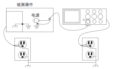
Figure 5 Complete ground circuit or ground loop of the oscilloscope, probe, and test circuit on two different power outlets
In ground-loop noise injection, the noise is usually line-frequency noise (50 or 60 Hz)But usually, the noise may take the form of spikes or bursts, which are caused by building equipment such as air conditioners, switches, etc.
Various measures can be taken to avoid or minimize ground-loop noise problems. The first method is to use the same power circuit for the oscilloscope and the circuit under test to minimize the ground loop. In addition, the probe and its cable should be kept away from potential noise sources. In particular, do not route the probe cable alongside or across equipment power cables.
If a ground-loop noise problem persists, it may be necessary to short-circuit the ground loop by one of the following methods:
1. Use a ground isolation monitor.
2. Use a power-line isolation transformer on the test circuit or oscilloscope.
3. Use an isolation amplifier to isolate the oscilloscope probe from the oscilloscope.
4. Use a differential probe for measurement ( Suppressing common-mode noise )。
Under no circumstances should the oscilloscope or test circuit be isolated by compromising the safety three-wire grounding system. If a floating measurement is necessary, use a manufacturer-approved isolation transformer, preferably a ground isolation monitor designed specifically for the oscilloscope.
Note: To avoid electric shock, always connect the probe to the oscilloscope or probe isolator before connecting the probe to the circuit under test.
Induced noise
Noise can enter the common grounding system by being induced into the probe cable, especially when using a probe with a long cable. Proximity to power lines or other current-carrying conductors may cause current flow in the probe's outer cable shield. A circuit is formed through the building system common ground. To minimize this potential noise source, use a probe with a shorter cable when possible, and always keep the probe cable away from possible interference sources.
Noise can also be induced directly into the probe ground lead, a typical result of the probe ground lead; when connected to the test circuit, it behaves as a single-turn loop antenna. This ground-lead antenna is particularly susceptible to electromagnetic interference caused by logic circuits or other rapidly changing signals. If the probe ground lead is positioned too close to specific areas on the board under test, such as clock lines, the ground lead may pick up signals and mix them with the signal at the probe tip.
When noise is seen on the oscilloscope display for a signal, the question is whether this noise occurs as part of the signal at the probe tip or is induced in the probe ground lead.
To answer this question, try moving the probe ground lead. If the noise signal level changes, the noise is a signal induced into the ground lead.
Another very effective method for identifying noise sources is to disconnect the probe from the circuit and clip the probe ground lead to the probe tip. Then move this probe head back and forth along the circuit. / Ground-loop antenna. This loop antenna will pick up areas in the circuit that radiate noise strongly. Figure 6illustrates that, by connecting the probe ground lead to the probe tip and performing a search, it is possible to find which noise sources are present on a logic circuit board.

Figure 6 Example of noise induced on a circuit board in the probe ground loop (probe head shorted to the ground clip)
To minimize noise induced into the probe ground, keep the ground lead away from noise sources on the board under test. In addition, shortening the ground lead reduces the amount of noise picked up.
Reprinted from Tektronix

PCIM Europe 2026, Nuremberg: IWATSU and PMK at Booth H7-157
2026-06-15
APEC 2026: 41st IEEE Applied Power Electronics Conference and Exposition
2026-03-15
Semicon China 2026, Shanghai New International Expo Centre (SNIEC)
2026-03-11
WiPDA Asia 2025, Beijing International Convention Center, 15 August
2025-08-06